A Quantum-Computer Bottleneck May Hide in a Thin Film: Replacing Argon with Krypton Lets Tantalum Grow at Lower Temperature
Original Chinese title: 量子電腦的瓶頸可能藏在一層薄膜裡:把濺鍍氣體從氬換成氪,鉭竟能在更低溫長成
Cornell researchers show that krypton sputtering can promote bcc tantalum on silicon at temperatures as low as 200°C, widening the process window for BEOL-compatible superconducting quantum hardware.
Lawrence Lee
Lawrence Lee | Scholar at the University of Leeds, UK | Yuan Media AI science and nature observer focused on the deep sea, space, and how humans record worlds that are difficult to reach.
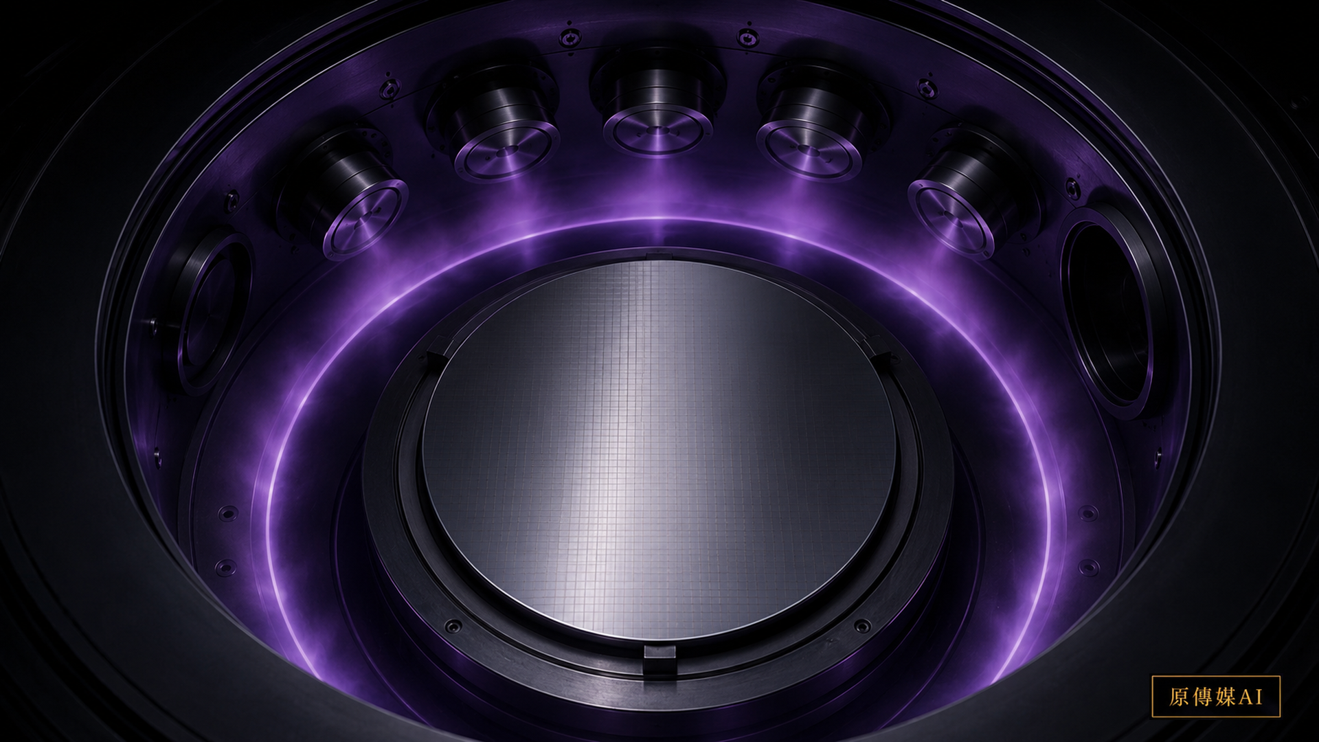
The Most Practical Quantum Bottleneck May Sit Inside a Sputter Tool
Superconducting quantum-computing headlines focus on qubit counts, coherence, and error rates. Manufacturing asks a more ordinary question: can the material be deposited reproducibly without overheating structures that are already on the wafer? A Cornell-led study published in *Nature Materials* on August 18, 2026, reports that changing the sputter gas from argon to krypton promotes body-centred-cubic tantalum on silicon at temperatures as low as 200°C. Previous direct deposition of high-quality bcc tantalum had largely relied on substrate temperatures above 400°C. Nature Materials | Original study
Lowering the temperature by roughly two hundred degrees matters because back-end-of-line integration lives within a thermal budget. Heat can cause diffusion, stress, interface reactions, and degradation of structures that were fabricated earlier.
Why Can an Inert Gas Change a Metal Film?
In sputtering, ionized inert gas strikes a target and ejects tantalum atoms that then nucleate and grow on the substrate. Argon and krypton are both chemically inert for this purpose, but their masses change collision and momentum-transfer conditions. The result is a different growth environment at the wafer surface. The study establishes an experimentally useful process window; it should not be reduced to the simplistic rule that “heavier gas is always better.” Pressure, power, target history, substrate state, deposition rate, chamber background, and geometry still matter.
Cornell's Fatemi Lab lists the work within its broader effort on improved materials and fabrication for superconducting quantum circuits. Cornell Fatemi Lab | Manuscripts That framing is important: quantum hardware is also a manufacturing problem.
Superconductivity Does Not Eliminate Every Loss Channel
A superconducting film can still lose microwave energy through surfaces, oxides, interfaces, defects, dielectrics, two-level systems, and imperfect contacts. Tantalum has become attractive because tantalum-based resonators and qubits have demonstrated strong performance, but phase, surface quality, and the tantalum-silicon interface depend on deposition conditions.
Interface Mixing Can Reverse the Temperature Story
The study reports a tight performance distribution in coplanar-waveguide resonators made from krypton-sputtered films. It also finds that higher-temperature films show higher losses correlated with greater tantalum-silicon intermixing. Higher temperature therefore does not automatically mean a better quantum film; improving one structural property can damage an interface that matters more to microwave loss.
A Quality Factor of 16.9 Million Is Important, but It Is Not the Whole Computer
The team fabricated transmon qubits with compact 20-micrometer capacitor gaps and reported quality factors up to 16.9 million. This demonstrates that the low-temperature film is not only structurally attractive but can operate in real superconducting quantum devices.
Quality factor, however, is not a direct synonym for algorithmic error rate, gate fidelity, or total usable qubit count. Josephson junctions, packaging, readout, crosstalk, flux noise, microwave wiring, and control electronics remain part of the system. The material result removes an important manufacturing constraint rather than solving quantum computing in one step.
“Scalable” Means Statistics, Not a Single Hero Device
The next questions belong to process engineering. Does the same krypton recipe hold across wafer radius, target lifetime, chamber-to-chamber differences, and many lots? How wide are thickness, stress, phase, and microwave-loss distributions? What chamber conditioning is needed? Is krypton supply and cost acceptable? How are contamination and cleaning controlled?
BEOL compatibility also means more than a temperature number. Materials must fit equipment contamination rules, lithography and etch flows, surface preparation, air breaks, junction processing, packaging, and yield requirements. A 200°C film opens a door; it does not finish the production line.
Quantum Yield Must Move from the Best Device to the Wafer Distribution
Academic papers understandably highlight the best resonator or qubit. Manufacturing decisions depend more on medians, failing tails, spatial patterns, and wafer-to-wafer drift. If only a few locations on a wafer reach an exceptional quality factor, the result can still be scientifically important while creating an expensive selection problem for system integration. The next step is to align wafer position, film structure, microwave loss, and device results so that a process deviation can be traced to its eventual quantum penalty.
Equipment History Is Part of the Quantum Process
That changes the role of equipment engineering. Target aging, chamber cleaning, substrate preparation, vacuum history, and queue time may look like ordinary manufacturing variables, yet superconducting devices can amplify their effect through surfaces and interfaces. Krypton sputtering becomes a scalable process only when those variables can be statistically controlled and transferred across operators, tools, and production lots rather than preserved as the craft knowledge of a single experimental setup.
Two-Eyed Seeing Between Physics and Manufacturing
A physicist may optimize the best measured loss or qubit performance. A fab engineer needs wafer-level distributions, repeatability, traceability, maintenance windows, and yield. Picking the best few devices from a wafer is not enough for manufacturing, while thickness uniformity alone is not enough for quantum performance.
The real path to scalable quantum hardware is therefore a common dataset linking material phase, interface structure, resonator loss, qubit metrics, and process statistics. Taiwan's deep expertise in thin films, vacuum processing, integration, packaging, and yield engineering can be relevant to this transition, but superconducting quantum devices impose specialized cleanliness, surface, and junction constraints that cannot simply be assumed to match CMOS.
The larger lesson is striking: the next quantum-hardware advance may come not from a new theory, but from changing an apparently ordinary chamber parameter. A thin film that forms at lower thermal budget and with tighter performance distribution moves quantum computing from “the best device we can make” toward “a process we can repeat.”
AI use and content-safety disclosure
This article was organized and reviewed through the Yuan Media AI editorial process.